Combined BEM/FEM Resistance Modeling of Stratified Substrates
Technical Papers - Submicron IC Extraction
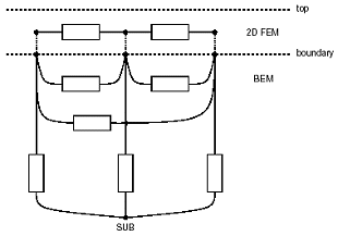
Combined BEM/FEM Resistance Modeling of Stratified Substrates With Layout-Dependent Doping Patterns in the Top Layer
REFERENCE NUMBER: I02-WP2005
AUTHORS: E. Schrik, A.J. van Genderen, and N.P. van der Meijs
VENUE: Discussion paper, 2005, Delft, The Netherlands
ABSTRACT - In present-day micro-electronic designs, the impact of substrate noise is becoming ever more important. Therefore, it is of great importance to acquire an acurate model of substrate coupling effects. Basically, such a model can be obtained by discretizing the substrate with either a Finite Element Method (FEM) or a Boundary Element Method (BEM). The FEM is the most versatile and flexible whereas the BEM is faster, but requires a stratified, layout-independent doping profile for the substrate. Thus, the BEM is unable to properly model any specific, layout-dependent doping patterns that are usually present in the top layers of the substrate, such as channel stop layers. This paper describes a way to incorporate these doping patterns into our substrate model by combining a BEM for the stratified doping profiles with a 2D FEM for the top-level, layout-dependent doping patterns. The result is initially a detailed netlist that can be reduced by a gaussian elimination procedure which is usually employed for interconnect. The method has been implemented in the SPACE layout to circuit extractor and it has been successfully verified with an alternative modeling tool.

To obtain a copy of this paper please make a note of the reference number and fill out ourrequest form.
Back to alltechnical papers.
