OptEM Package - Post-layout Verification Software for Advanced IC Package Interconnects
OptEM Package
OptEM Package
OptEM Package is a post-layout verification software tool for the extraction, electromagnetic analysis, and modeling of advanced IC package interconnects.

Product Description
Miniaturization and portability both contribute to driving package technology forward. Smaller size requirements - the need to fit more functionality into less area - affect the I/O pin count, reliability, and processes used to generate the package. Portability requirements affect the weight and materials of the package. And all factors can affect the integrity of the signal passing through the package leads. OptEM Package is a CAE software tool that offers a unique solution for modeling the interconnects of a package.
Interconnect Analysis
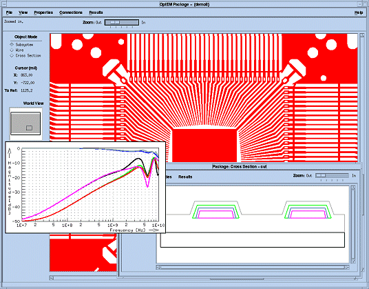
OptEM Package is a post-layout verification tool for the extraction, electromagnetic analysis, and modeling of advanced IC package interconnects. The software reads DXF or GDSII design files, and combines this layout data with physical process information to generate optimized SPICE models for any number of package traces in the design. With its 2D and 3D electromagnetic analysis, OptEM Package is able to accurately calculate resistance, capacitance, inductance, and conductance in matrix format, S-parameters, complex characteristic impedance, and plot the current distribution and time delay data for the interconnects.
Physical Process Specification
Manufacturing multi-material leads using plating and bonding techniques involves a number of physical process specifications. OptEM Package allows you to build different technology files by specifying layers of conducting ferromagnetic and dielectric materials. Different material combinations like metal-on-metal and conformal layers can be built to represent pins in packages, vias, and pad layers. In order to optimize design time all technology files can be re-used in other OptEM software applications.
Package Modeling Facility
Ball grid arrays (BGAs), chip scale packages (CSPs), pin grid arrays (PGAs), and lead frames represent some of the types of packages that can be analyzed by OptEM Package. The electromagnetic analysis performed by the software also includes both conductor and dielectric losses which can affect the R, L, C, and G of the package leads. Accurate parasitic calculations are necessary for calculating signal integrity results. The analysis results are then used by the software to automatically build parasitic reports with full R L C G and Zo matrices, S-parameter models, frequency-dependent SPICE models, current distribution and timing data plots.

Features & Benefits
Features
- reads DXF and GDSII files
- allows for trace enlargements, over/undercutting, and conformal layer geometries due to the manufacturing process
- automatic via connection and external port placement capability when set up in the process technology files
- variables for geometric, material, and frequency parameters
- conductor plating on wires
- frequency-dependent analysis with inclusion of conductor losses (due to proximity and skin effects) and dielectric losses (typical for semiconductors)
- batch analysis
- generates flexible parametric reports that include R, L, C, G and Zo values
Benefits
- uses standard manufacturing files
- accommodates physical process specifications which include deposition and etching processes
- extracts entire net quickly and efficiently based on layout and physical properties
- ability to define frequency dependent materials
- models pins in packages
- provides accurate results taking into account today's technologies
- allows concurrent modeling and analysis
